Resistive Random Access Memory (ReRAM) is a next-generation memory technology under development. After years of setbacks, the technology has finally begun to be welcomed.
Fujitsu and Panasonic are jointly investing in the development of second-generation ReRAM devices. In addition, Crossbar is experimentally producing a 40nm ReRAM technology, which is currently being produced by SMIC's fab in China. TSMC and UMC are not outdone, and ReRAM has recently been added. I have developed my own roadmap and will develop this technology for my clients around the next year.
For many years, people have been touting ReRAM, saying it is a replacement for traditional memory technologies such as NAND, but ReRAM is more difficult to develop than anyone predicted. In addition, NAND has evolved farther than previously thought, leading many companies to delay or even terminate their ReRAM development.
Not all chip manufacturers support ReRAM. Some companies, such as GlobalFoundries, are more chilly about ReRAM technology, but are developing different types of next-generation memory technologies.
Compared to flash memory, ReRAM has the advantage of lower read latency and faster write speed. In traditional memory, data is stored as a charge. In ReRAM, a voltage is applied to a stacked material, which in turn causes a change in resistance that can be recorded in memory (0 and 1).
Despite these excellent attributes, there are only a handful of companies that have shipped ReRAM so far. Other companies are still struggling because ReRAM technology is physically difficult. And in some cases, the performance and reliability of ReRAM did not meet expectations.
ReRAM does not replace NAND or other memory, but it will find its place, especially in embedded memory applications. YahokaeSheu, vice president of embedded non-volatile memory at UMC, said: "ReRAM is a cost-sensitive solution, such as wearable and IoT devices. ReRAM is suitable for some low-end MCUs and requires lower memory density. Consumer products."
But for future applications, the goal of some next-generation memory technologies such as ReRAM is the so-called storage-classmemory market. For many years, the memory industry has been looking for a new type of memory, storage-level memory. This memory can be used between the system's main memory (DRAM) and memory (NAND flash) to fill the growing latency gap between the two.
Another potential application for ReRAM is neuromorphic computing. Neuromorphic calculations use brain-inspired computational functions that can be used to implement artificial intelligence and machine learning. However, before ReRAM enters these markets, the memory industry must first control ReRAM on a small scale.
Why do you want to make next generation memory?
The memory industry has been developing ReRAM and other next-generation memory technologies for many years. Because of the many limitations of traditional memory, new memory types are expected to fill these gaps.
Er-XuanPing, general manager of AppliedMaterials Silicon Systems Group Memory and Materials, said: "They are solving DRAM and NAND problems. NAND is slow. DRAM is fast, but it is volatile."
DRAM is volatile, so when the system is powered down, its data is lost. The flash memory can continue to save data even when the power is turned off. However, in actual work, the flash memory will go through multiple rounds of read/write cycles, which is a slow process.
In general, the next generation of memory types are characterized by being fast, non-volatile and providing unlimited endurance. They also provide bit-writable, erasable features that make them a perfect replacement for DRAM and flash memory.
The problem with these memory technologies is that they rely on exotic materials and complex switching mechanisms, so next-generation memory types require longer development time. At the same time, the memory industry continues to extend DRAM and flash memory, making it difficult for new memory types to gain a foothold in the market.
However, there are several new memory types that are welcoming, with 3DXPoint and STT-MRAM being the strongest. There are also other types of carbon nanotube RAM, FRAM and ReRAM.
No single memory type is versatile and can handle all applications. Each technology has different properties and can perform different functions. David Fried, chief technology officer of Coventor, a subsidiary of LamResearch, said: "I expect these advanced memory technologies to be used first in applications that embody and leverage their unique advantages."
The 3DXPoint technology developed by Intel and Micron is the next generation of phase change memory. STT-MRAM uses the magnetism of electron spin to provide non-volatility.
Carbon nanotube RAM uses nanotubes to form a resistive state. FRAM uses ferroelectric capacitors to store data.
ReRAM is different from the above methods. In years of development and development, ReRAM became notorious in 2008, when Hewlett-Packard proposed a kind of ReRAM called memristor. For many years, HP has been developing a future-oriented system called TheMachine that integrates a memristor. But analysts say that after years of working on this technology, HP turned to a more traditional memory solution and withdrew from the path of memristors.
Now HP has started working with Western Digital to develop another ReRAM technology. Companies such as 4DS, Adesto, Crossbar, Micron, Panasonic, Samsung, and Sony are also developing ReRAM.
But so far, Panasonic is the only company that produces ReRAM in volume. In addition, Crossbar is also expected to start shipping ReRAM before the end of this year.
Other companies are still working hard to develop ReRAM. "Adesto has been slowly shipping low-density CBRAM, and they believe it will be shipped in volume in 2018." Web-FeetResearch CEO Alan Niebel said of conductive bridged RAM (CBRAM, a ReRAM), " Western Digital and HP are already in trouble, but may be able to ship in 2019."
At the same time, Sony is adjusting its own ReRAM development work. Sony and Micron have been working together to develop ReRAM for many years, but Micron has recently withdrawn from the project. In turn, he began to work with Intel to focus on developing 3DXPoint, leaving Sony without a fab partner to develop ReRAM.
In terms of foundries, SMIC, TSMC, and UMC are developing and/or providing ReRAM processes for OEM customers. But GlobalFoundries and Samsung have not yet introduced ReRAM.
Wafer foundries are exploring all next-generation memory types, but their focus is on technologies that are more likely to succeed in the long run. Dave Eggleston, vice president of embedded memory at GlobalFoundries, said: "The cost of investing in these technologies is high, and the industry can only invest so much."
For example, the technology that GlobalFoundries focuses on is STT-MRAM. Samsung, TSMC and UMC are also developing STT-MRAM for OEM customers. Eggletston said: "The most commercial potential of all these technologies is MRAM. Embedded MRAM is at the forefront. If you can get investment, other technologies will become more and more difficult to apply."
ReRAM has some advantages, but it still faces serious challenges. He added: "ReRAM is actually a bit disappointing in terms of adoption."
What is ReRAM?
ReRAM is also a difficult technology to master, but it is a relatively straightforward process for fab production. Both ReRAM and STT-MRAM require only a few mask steps and can be fabricated in a so-called post-production line (BEOL) manufacturing process in a fab. Moreover, both STT-MRAM and ReRAM are built on the contacts or vias of the metal layer of the chip.
It's one thing to make ReRAM, but it's another thing to make it work. In general, there are two main types of ReRAM - oxygen-vacancy ReRAM and CBRAM. Oxygen vacancies ReRAM is also known as oxide-based ReRAM (OxRAM).
Both OxRAM and CBRAM are two-terminal devices - consisting of a top electrode and a bottom electrode. Between the two electrodes is a switching medium.
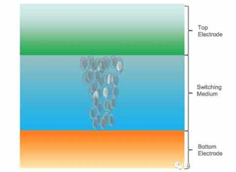
Figure 1: FilamentaryReRAM technology from Crossbar
In OxRAM, a metal oxide material is sandwiched between the two electrodes. When a positive voltage is applied to the top electrode, conductive filaments are formed between the two electrodes. These filaments are composed of ionic atoms.
These conductive filaments break when a negative voltage is applied to the bottom electrode. Therefore, the switching between the high and low resistance of the ReRAM is realized in effect. In memory, the change in resistance is expressed as 0 and 1.
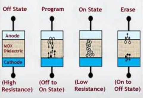
Figure 2: ReRAM at work, from Adesto
Similar to OxRAM, CBRAM also creates resistance states by building and destroying filaments. However, CBRAM injects copper or silver metal into silicon to form a conductive bridge or filament between the two electrodes.
Others are also studying the method of non-filament. Unlike forming filaments, this technique uses self-rectifying techniques to create switching effects. Some people classify this technology as OxRAM.
In any case, ReRAM technology is very difficult. ThorstenLill, vice president of LamResearch, said: "If you can develop it, ReRAM can really improve the read/write latency, but it has reliability limitations. Its unit switch will change its properties after tens of thousands of times. It seems It is related to the physicochemical effect of building filaments. We know very little about this."
DRAM and flash memory are processed electronically. OxRAM and CBRAM involve complex processes that control the formation of filaments by ion atoms. The electrons are lighter and the atoms are heavier.
“ReRAM looks simple on paper, but it’s not the case,†said Applied’s Ping. “When you move ions through the material, they not only form a current, but also an electric field that responds to it. Diffusion, temperature behavior, and electrical behavior must all be considered together. This necessarily involves dealing with many natural parameters. So it is very complicated."
Ping continues: "For example, when you input an electrical pulse to any kind of ReRAM, there will be RC interactions. Depending on the RC interaction, the locally generated heat will also be different and will not remain the same. If this is The difference is that the diffusion rate of oxygen will be different. This is a dilemma. On the one hand, the electrons may be too light. Then it will cause high noise. On the other hand, the atoms are too heavy. This is not simply electricity. Can solve it."
OxRAMvs.CBRAM
Matsushita began shipping ReRAM in 2013 and became the first company in the world to ship ReRAM. At that time, Panasonic introduced an 8-bit microcontroller (MCU) that integrates 180nm ReRAM as an embedded memory module.
Last year, Panasonic and Fujitsu jointly launched the second generation of ReRAM technology. Also based on the 180nm process, this 4Mbit ReRAM device is suitable for low power applications such as portable and medical products.
Now, Panasonic is currently developing 40nm ReRAM, and the goal is to launch it in 2018. A foundry of UMC is manufacturing this technology for Panasonic.
Panasonic's ReRAM is based on the OxRAM method. Panasonic chief engineer ZhiqiangWei said: "We think OxRAM's retention property is better than CBRAM."
At the 180nm node, Panasonic's ReRAM is based on a TaOx material with a Ta2O5stalking matrix. For comparison, Wei said that the 40nm node ReRAM will use "the same basic concept, but not exactly the same stacking method."
On the device side, Panasonic's ReRAM is designed around a 1T1R (single transistor single resistor) architecture. The 1T1R requires a large transistor to provide enough drive current for the device. This in turn limits the memory density of the chip.
But 1T1R is ideal for embedded memory applications. OEMs will use MCUs and other chips for embedded applications. In general, MCUs can integrate embedded memory on the same device. Embedded memory is typically based on EEPROM or NOR flash and can be used to store code and other data.
So what is the applicable field of ReRAM? In one case, the 4Mbit ReRAM from the Fujitsu-Panasonic package was denser than the EEPROM. In fact, ReRAM can replace EEPROM.
Therefore, the positioning of embedded ReRAM is a low power, cost sensitive solution that does not require fast write speeds. UMC's Sheu said: "ReRAM is positioned as a low-cost solution for the Internet of Things and other applications."
Currently ReRAM and similar rival STT-MRAM have different market positioning. "MRAM is aimed at applications that require higher performance, such as MCUs and cars," Sheu said. "We believe STT-MRAM can be an excellent non-volatile memory alternative in the future because it has better scalability. And performance."
In one application, the STT-MRAM is positioned to replace NOR in the MCU of the 22nm and later nodes. NOR is difficult to expand after the 28nm node and requires a new solution like STT-MRAM. Over time, ReRAM is also likely to become an alternative to NOR.
So far, STT-MRAM has been extended to 28nm, and 22nm and beyond are also being developed. Crossbar's ReRAM technology is at 40nm, and the technology at 28nm and beyond is still under development.
Instead of using the OxRAM method, the fabless startup Crossbar uses an electrochemical metallization process. According to experts, from a mechanical point of view, this process uses metal ion filaments close to CBRAM.
"The problem with OxRAM is that it's difficult to scale," said Sylvain Dubois, vice president of marketing and business development at Crossbar. "It regulates the filaments inside the unit. The switch ratio (on/offratio) is not very good."
For its own electrochemical solution, Crossbar claims that the on/off ratio will increase with expansion. Dubois said: "This means that this technology will improve as you expand to the next process node."
Therefore, Crossbar's ReRAM devices can be extended beyond the 40nm node. He said: "Now we are working with a 20-nanometer wafer foundry and even a 10-nm foundry partner."
More importantly, Crossbar's ReRAM has lower read latency and faster write performance than flash. To take advantage of the technology that it has already brought to market, Crossbar is developing two architectures, the 1T1R and a stacked memory device.
Crossbar's 1T1R technology targets the embedded world. Its first 1T1R product is based on the 40nm process and is produced by SMIC.
Crossbar is also developing a technology for storage-level memory applications. This architecture consists of a single layer that is stacked on the device. A selector is built in to allow one transistor to drive one or thousands of memory cells.

Figure 3: Crossbar's stacked memory architecture from Crossbar
Dubois said: "At the 16nm node, we only need four layers, we can get a density of 32GB. With fewer layers, we can reach the GB level."
Crossbar's stacked configuration of ReRAM targets SSDs and dual in-line memory modules. For these applications, ReRAM is often used with existing memory. It may also replace some DRAM and NAND.
He said: "I don't think we will replace a category overnight. We are going to open up new ways of accessing data. So we are not planning to replace plug-and-play flash or DRAM. Instead, they are used in them. between."
ReRAM is still promising in embedded applications, but in the storage-class memory space, this technology will face a lot of competition. Applied's Ping said: "It faces competition from existing solutions. This ecosystem is controlled by a larger supplier, so it is not easy."
In addition, bringing a new memory technology to market requires a lot of resources. For example, Intel and Micron are pushing 3DXPoint technology, and of course they have the resources to open the way for their business.
future
Although the success of ReRAM in the storage-class memory market remains to be seen, this technology can be used in other areas, especially neural networks.
Some companies, such as Facebook and Google, have developed machine learning systems that use neural networks. Neural networks can help the system process data and identify patterns. Then, it can learn what attributes are important.
Many of these systems use FPGAs and GPUs with SRAM-based memory. The memory industry is developing ReRAM for this area. ReRAM is much denser than the GPU/SRAM architecture.
The calculation using dedicated hardware such as ReRAM is also called neural morphology calculation. Ping said: "The neurological morphology is analog. OxRAM has such a property. Its resistance can be changed to meet the needs of neuromorphic calculations."
But neuromorphic systems require cascading multiple stacked ReRAM devices. As mentioned earlier, it is already difficult to control a single ReRAM device.
Controlling multiple ReRAMs is even more difficult. Ping said: "The neuromorphic calculation will eventually require some control over the resistance. Similarly, when using ReRAM, you have to move the atoms in the filament. So there are many possibilities in this area. This is still unknown."
Editor in charge: Malan
Women's suits are mainly divided into two types: suit trousers and suit skirts. This is mainly selected according to everyone's own preferences. The trousers make people look cooler, and the trousers make people look more sexy. The color of the upper and lower parts of the suit should be the same. The best colors for professional suits are black, navy, taupe, gray, and dark red. Delicate checkered, printed stripes are acceptable; however, black is the most common in college clubs. Women's formal skirts are mainly narrow skirts. Young women's skirts can choose to have a hem of 3-6 cm above the knee, but not too short; leather or imitation leather suit skirts are not suitable for formal occasions; sometimes you will see some It is not advisable to wear an A-group under a girl's shoes and suits on formal occasions. For example, going to formal occasions such as spring/autumn training and regional competitions will be very rude.
Lady'S Blazer ,Black And White Blazer Womens,Dark Green Blazer Womens,Fitted Womens Blazer
NINGBO DHK IMPORT & EXPORT CO., LTD , https://www.deheke.com